Introduction
In today’s high-speed electronic designs, signal integrity has become a critical factor determining the success or failure of a product. As data rates continue to increase and component densities rise, the importance of proper PCB stackup design cannot be overstated. A well-designed stackup serves as the foundation for good signal integrity, electromagnetic compatibility, and overall electrical performance. Companies like RAYMING PCB have recognized this challenge and developed specialized expertise in creating optimized stackups for demanding applications.
This article explores the essential considerations, methodologies, and best practices for optimizing PCB stackups to achieve superior signal integrity in your designs. Whether you’re working on high-speed digital circuits, sensitive analog systems, or mixed-signal applications, these principles will help ensure your signals remain clean and reliable throughout your board.
Understanding the Fundamentals of PCB Stackup
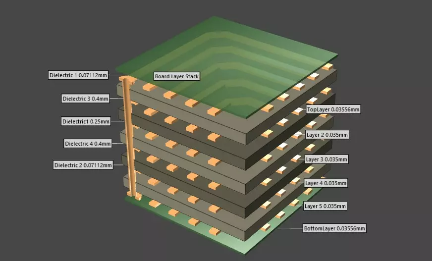
A PCB stackup refers to the arrangement of copper layers and dielectric materials that make up a printed circuit board. It defines the number of layers, their thicknesses, material properties, and spacing. RAYMING PCB and other industry leaders emphasize that an effective stackup design begins with understanding these fundamental components:
Copper Layers
Copper layers serve as conductors for your circuit traces and planes. Their thickness (typically measured in ounces per square foot) affects impedance, current-carrying capacity, and thermal management. In high-speed designs, RAYMING PCB often recommends using thicker copper for power planes (1oz or 2oz) while maintaining thinner copper (0.5oz or 1oz) for signal layers to achieve better impedance control.
Dielectric Materials
The insulating materials between copper layers significantly impact signal integrity. Key properties include:
- Dielectric constant (Dk): Affects signal propagation speed and impedance
- Dissipation factor (Df): Determines signal loss
- Glass weave style: Impacts dielectric constant consistency across the board
RAYMING PCB offers various high-performance materials like Isola FR408HR, Rogers, and Megtron for critical signal integrity applications. These materials feature lower loss tangents and more stable dielectric constants across frequency and temperature ranges compared to standard FR-4.
Prepreg and Core
The dielectric material comes in two forms:
- Core: A fully cured fiberglass-reinforced resin with copper on both sides
- Prepreg: Partially cured resin sheets that bond cores together during lamination
Understanding the differences in thickness tolerances and Dk values between these materials is crucial for accurate impedance calculations. RAYMING PCB’s engineering team works closely with designers to select the optimal combination of cores and prepreg for specific applications.
Key Factors Affecting Signal Integrity in PCB Stackups
Impedance Control
Controlled impedance is perhaps the most critical factor in high-speed design. Common target impedances include 50Ω for single-ended traces and 85Ω or 100Ω for differential pairs. RAYMING PCB’s impedance modeling software allows for precise calculation of trace geometries required to achieve target impedances based on:
- Trace width
- Copper thickness
- Dielectric thickness
- Dielectric constant
- Reference plane proximity
Return Path Management
Every signal requires a return path. In high-frequency designs, the return current follows the path of least impedance (not necessarily the path of least resistance). This typically means it flows directly beneath the signal trace on the nearest reference plane. RAYMING PCB’s stackup consultants recommend:
- Placing signal layers adjacent to continuous ground planes
- Minimizing the distance between signal traces and their reference planes
- Avoiding splitting reference planes under high-speed signals
- Using ground planes rather than power planes as references when possible
Layer Pairing and Symmetry
A symmetrical stackup helps prevent board warpage during manufacturing and thermal cycling. RAYMING PCB typically designs stackups with the following considerations:
- Balanced copper distribution across the centerline
- Paired routing layers with similar trace density and orientation
- Even number of layers when possible
- Alternating signal and plane layers for improved isolation
Loss Minimization
Signal loss degrades performance in high-speed designs through:
- Dielectric loss: Absorption of signal energy by the insulating material
- Conductor loss: Resistive losses in the copper traces
- Radiation loss: Energy lost through electromagnetic radiation
RAYMING PCB addresses these concerns by offering low-loss materials, optimizing trace geometries, and using proper reference planes to contain electromagnetic fields.
Practical Stackup Configurations for Different Applications
4-Layer Stackup for General-Purpose Designs
A basic 4-layer stackup typically follows this arrangement:
- Signal (Top)
- Ground plane
- Power plane
- Signal (Bottom)
While economical, this configuration has limitations for high-speed signals. RAYMING PCB often recommends enhancements such as:
- Using thicker dielectric between layers 2-3 to improve impedance control
- Carefully planning power distribution to minimize loops
- Limiting high-speed signals to the outer layers with direct ground references
6-Layer Stackup for Medium-Complexity Designs
A 6-layer stackup offers improved performance:
- Signal (Top)
- Ground plane
- Signal (Inner)
- Power plane
- Signal (Inner)
- Ground plane
- Signal (Bottom)
This configuration, frequently used by RAYMING PCB for mixed-signal designs, provides better isolation between analog and digital sections while maintaining reasonable manufacturing costs.
8+ Layer Stackup for High-Speed Applications
For demanding applications, RAYMING PCB recommends 8 or more layers:
- Signal (Top)
- Ground plane
- Signal (Inner)
- Ground plane
- Power plane
- Ground plane
- Signal (Inner)
- Ground plane
- Signal (Bottom)
This approach provides excellent signal integrity through:
- Signal layers always adjacent to reference planes
- Improved power distribution with dedicated planes
- Better isolation between signal groups
- Reduced crosstalk through increased layer separation
Advanced Techniques for Enhanced Signal Integrity
Embedded Stripline vs. Microstrip
RAYMING PCB offers both stripline (signals embedded between planes) and microstrip (signals on outer layers) configurations. Each has advantages:
Microstrip:
- Easier to fabricate with tighter tolerances
- Better heat dissipation
- Easier to access for probing and modification
Stripline:
- Better shielding from external interference
- Reduced emissions
- Less susceptible to environmental factors
- Better crosstalk control
For the most demanding applications, RAYMING PCB often recommends dual-stripline configurations where signal layers are sandwiched between dedicated ground planes.
Handling Mixed Signal Requirements
Modern PCBs frequently contain both high-speed digital and sensitive analog circuits. RAYMING PCB’s engineers recommend these approaches for mixed-signal stackups:
- Segregate analog and digital ground planes on separate layers
- Connect grounds at a single point or through filtered connections
- Place high-speed digital signals on stripline layers for better containment
- Position analog signals away from digital power planes
- Use buried capacitance for improved power integrity
Managing Differential Pairs
Differential signaling provides excellent noise immunity but requires careful stackup design. RAYMING PCB ensures differential integrity by:
- Maintaining tight coupling between pair members
- Providing clear return paths for both traces
- Controlling differential impedance through precise modeling
- Minimizing skew by routing pairs on the same layer
- Using edge-coupled configurations in layers with appropriate spacing
RAYMING PCB’s Approach to Stackup Optimization
RAYMING PCB has developed a systematic approach to stackup design:
- Requirements Analysis: Understanding the specific needs of each design, including speed, density, cost constraints, and performance targets.
- Material Selection: Choosing appropriate base materials, prepregs, and cores based on electrical, thermal, and mechanical requirements.
- 2D Field Solver Simulation: Using advanced electromagnetic simulation tools to verify impedance profiles and analyze field distributions.
- Manufacturability Review: Ensuring the stackup can be reliably produced within tolerance specifications.
- Prototype Validation: Building and testing representative test coupons to verify actual impedance values match target specifications.
This methodical approach has enabled RAYMING PCB to successfully produce high-performance boards for telecommunications, medical devices, aerospace, and other demanding industries.
Practical Implementation Guidelines
Documentation Standards
When working with RAYMING PCB, providing clear stackup requirements helps ensure successful implementation:
- Target impedances for each signal type
- Maximum acceptable tolerance ranges
- Critical signals requiring special consideration
- Regulatory requirements for the final product
Verification Techniques
RAYMING PCB employs several methods to verify stackup performance:
- Time Domain Reflectometry (TDR) for impedance verification
- Cross-sectional analysis to confirm layer thicknesses
- Vector Network Analyzer (VNA) measurements for insertion and return loss
- Eye diagram analysis for digital signal quality assessment
Conclusion
Optimizing PCB stackup for signal integrity requires a comprehensive understanding of electrical, mechanical, and manufacturing considerations. As signal speeds continue to increase, the importance of thoughtful stackup design becomes ever more critical to product success.
RAYMING PCB’s expertise in advanced materials, impedance modeling, and manufacturing processes provides designers with a valuable resource for creating high-performance electronic systems. By applying the principles outlined in this article and leveraging partnerships with experienced fabricators like RAYMING PCB, engineers can develop stackup designs that deliver excellent signal integrity even in the most demanding applications.
Whether you’re working on high-speed digital interfaces, sensitive analog circuits, or complex mixed-signal systems, a properly optimized stackup forms the foundation upon which reliable electronic products are built. Take the time to get this fundamental aspect of your design right, and the benefits will cascade throughout your entire system’s performance.